stm32f407探索者开发板(十一)——SystemInit时钟系统初始化剖析
·
文章目录
一、回顾
SYSCLK主要是用PLLCLK作为时钟源
二、SystemInit
systeminit是在main函数调用之前进行的
void SystemInit(void)
{
  /* FPU settings ------------------------------------------------------------*/
  #if (__FPU_PRESENT == 1) && (__FPU_USED == 1)
    SCB->CPACR |= ((3UL << 10*2)|(3UL << 11*2));  /* set CP10 and CP11 Full Access */
  #endif
  /* Reset the RCC clock configuration to the default reset state ------------*/
  /* Set HSION bit */
  RCC->CR |= (uint32_t)0x00000001;

  /* Reset CFGR register */
  RCC->CFGR = 0x00000000;

  /* Reset HSEON, CSSON and PLLON bits */
  RCC->CR &= (uint32_t)0xFEF6FFFF;

  /* Reset PLLCFGR register */
  RCC->PLLCFGR = 0x24003010;

  /* Reset HSEBYP bit */
  RCC->CR &= (uint32_t)0xFFFBFFFF;

  /* Disable all interrupts */
  RCC->CIR = 0x00000000;

#if defined (DATA_IN_ExtSRAM) || defined (DATA_IN_ExtSDRAM)
  SystemInit_ExtMemCtl();
#endif /* DATA_IN_ExtSRAM || DATA_IN_ExtSDRAM */

  /* Configure the System clock source, PLL Multiplier and Divider factors,
     AHB/APBx prescalers and Flash settings ----------------------------------*/
  SetSysClock();

  /* Configure the Vector Table location add offset address ------------------*/
#ifdef VECT_TAB_SRAM
  SCB->VTOR = SRAM_BASE | VECT_TAB_OFFSET; /* Vector Table Relocation in Internal SRAM */
#else
  SCB->VTOR = FLASH_BASE | VECT_TAB_OFFSET; /* Vector Table Relocation in Internal FLASH */
#endif
}
2.1 FPU settings
/* FPU settings ------------------------------------------------------------*/
  #if (__FPU_PRESENT == 1) && (__FPU_USED == 1)
    SCB->CPACR |= ((3UL << 10*2)|(3UL << 11*2));  /* set CP10 and CP11 Full Access */
  #endif
浮点运算设置
2.2 Reset the RCC clock configuration to the default reset state(RCC时钟的初始化状态)
关闭RCC一些功能
  /* Reset the RCC clock configuration to the default reset state ------------*/
  /* Set HSION bit */
  RCC->CR |= (uint32_t)0x00000001; //CR寄存器选择时钟源,将最低位设置为1

  /* Reset CFGR register */
  RCC->CFGR = 0x00000000; //

  /* Reset HSEON, CSSON and PLLON bits */
  RCC->CR &= (uint32_t)0xFEF6FFFF;

  /* Reset PLLCFGR register */
  RCC->PLLCFGR = 0x24003010;

  /* Reset HSEBYP bit */
  RCC->CR &= (uint32_t)0xFFFBFFFF;

  /* Disable all interrupts */
  RCC->CIR = 0x00000000;
CR寄存器最低位使能
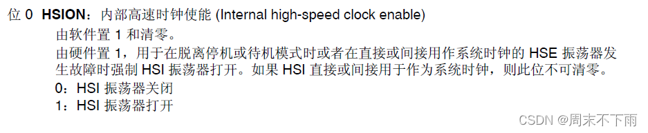
几点说明:Set就是打开,设置为1;Reset就是关闭,设置为0
如:
  /* Reset HSEON, CSSON and PLLON bits */
  RCC->CR &= (uint32_t)0xFEF6FFFF;
  //1111 1110 1111 0110 1111 1111 1111 1111
  //从0位开始,设置为0的,依次是第16位、第19位、第24位



也就是HSEON, CSSON and PLLON这三位设置为0,关闭
CSS是安全系统,如果调用的外部时钟挂了,将会切换到HSI时钟源上。
2.3 SetSysClock()
2.3.1 对HSE寄存器进行使能
  /* Enable HSE */
  RCC->CR |= ((uint32_t)RCC_CR_HSEON);
  //#define  RCC_CR_HSEON                        ((uint32_t)0x00010000)
  //位16是HSEON
使能HSE
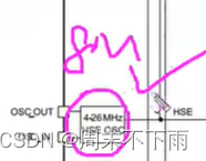
之后就要等待HSE稳定,即:
  /* Wait till HSE is ready and if Time out is reached exit */
  do
  {
    HSEStatus = RCC->CR & RCC_CR_HSERDY;
    StartUpCounter++;
  } while((HSEStatus == 0) && (StartUpCounter != HSE_STARTUP_TIMEOUT));

  if ((RCC->CR & RCC_CR_HSERDY) != RESET)
  {
    HSEStatus = (uint32_t)0x01;
  }
  else
  {
    HSEStatus = (uint32_t)0x00;
  }
2.3.2 对PWR_CR电源控制寄存器设置
    /* Select regulator voltage output Scale 1 mode */
    RCC->APB1ENR |= RCC_APB1ENR_PWREN;
    PWR->CR |= PWR_CR_VOS;
自己找手册翻吧,老师也没说清楚
2.3.3 对 RCC_CFGR寄存器操作
    /* HCLK = SYSCLK / 1*/
    RCC->CFGR |= RCC_CFGR_HPRE_DIV1;
//#define  RCC_CFGR_HPRE_DIV1                  ((uint32_t)0x00000000)        /*!< SYSCLK not divided */
#if defined (STM32F40_41xxx) || defined (STM32F427_437xx) || defined (STM32F429_439xx)
    /* PCLK2 = HCLK / 2*/
    RCC->CFGR |= RCC_CFGR_PPRE2_DIV2;

    /* PCLK1 = HCLK / 4*/
    RCC->CFGR |= RCC_CFGR_PPRE1_DIV4;
#endif /* STM32F40_41xxx || STM32F427_437x || STM32F429_439xx */

#if defined (STM32F401xx)
    /* PCLK2 = HCLK / 2*/
    RCC->CFGR |= RCC_CFGR_PPRE2_DIV1;

    /* PCLK1 = HCLK / 4*/
    RCC->CFGR |= RCC_CFGR_PPRE1_DIV2;
#endif /* STM32F401xx */
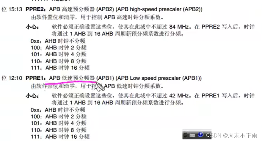
/* HCLK = SYSCLK / 1*/就是直接等于,那个预分频器赋为1,值为0
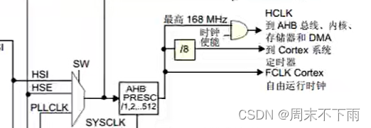
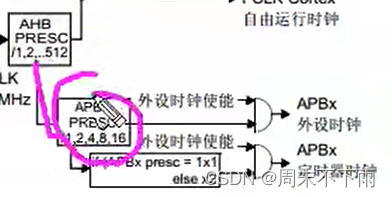
    /* PCLK2 = HCLK / 2*/
    RCC->CFGR |= RCC_CFGR_PPRE2_DIV2;

    /* PCLK1 = HCLK / 4*/
    RCC->CFGR |= RCC_CFGR_PPRE1_DIV4;
2.3.4 对PLLCFGR寄存器设置
主要是分频器、倍频系数
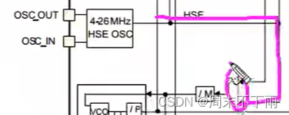
    /* Configure the main PLL */
    RCC->PLLCFGR = PLL_M | (PLL_N << 6) | (((PLL_P >> 1) -1) << 16) |
                   (RCC_PLLCFGR_PLLSRC_HSE) | (PLL_Q << 24);
//#define  RCC_PLLCFGR_PLLSRC_HSE              ((uint32_t)0x00400000)
//第22位,根据下图也就是选择器选择HSE作为时钟源

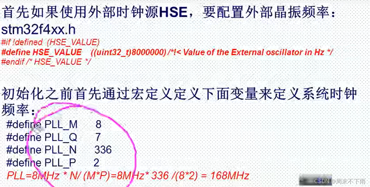
之后就是对位的一些宏定义,计算出来就是168M
#if defined (STM32F40_41xxx) || defined (STM32F427_437xx) || defined (STM32F429_439xx) || defined (STM32F401xx)
/* PLL_VCO = (HSE_VALUE or HSI_VALUE / PLL_M) * PLL_N */
#define PLL_M      8
#else /* STM32F411xE */
#if defined (USE_HSE_BYPASS)
#define PLL_M      8
#else /* STM32F411xE */
#define PLL_M      16
#endif /* USE_HSE_BYPASS */
#endif /* STM32F40_41xxx || STM32F427_437xx || STM32F429_439xx || STM32F401xx */

/* USB OTG FS, SDIO and RNG Clock =  PLL_VCO / PLLQ */
#define PLL_Q      7

#if defined (STM32F40_41xxx)
#define PLL_N      336
/* SYSCLK = PLL_VCO / PLL_P */
#define PLL_P      2
#endif /* STM32F40_41xxx */
之后就是使能主PLL
    /* Enable the main PLL */
    RCC->CR |= RCC_CR_PLLON;

    /* Wait till the main PLL is ready */
    while((RCC->CR & RCC_CR_PLLRDY) == 0)
    {
    }
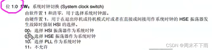
2.3.5 选择主PLL作为系统时钟源
    /* Select the main PLL as system clock source */
    RCC->CFGR &= (uint32_t)((uint32_t)~(RCC_CFGR_SW));
    RCC->CFGR |= RCC_CFGR_SW_PLL;
//#define  RCC_CFGR_SW_PLL                     ((uint32_t)0x00000002)        /*!< PLL selected as system clock */

    /* Wait till the main PLL is used as system clock source */
    while ((RCC->CFGR & (uint32_t)RCC_CFGR_SWS ) != RCC_CFGR_SWS_PLL);
    {
    }
三、小结
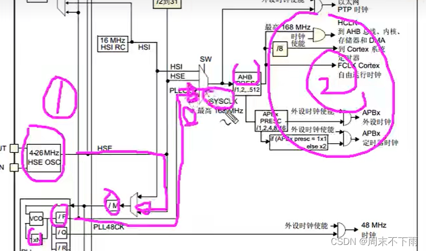
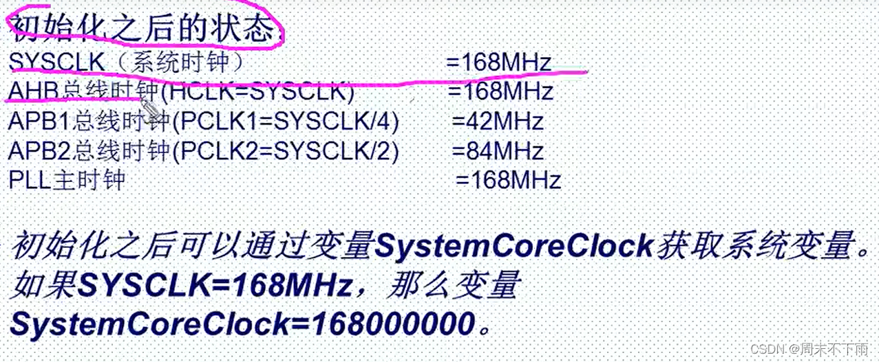
宏定义计算

北京人形旗下天工造物具身智能开源社区,聚焦具身天工与慧思开物两大平台
更多推荐
 0
0 0
0- 0


 已为社区贡献11条内容

所有评论(0)